Guides / Materials
Yttria Ceramic in Plasma Etch Chambers: Why It Replaces Alumina and Quartz
October 28, 2026
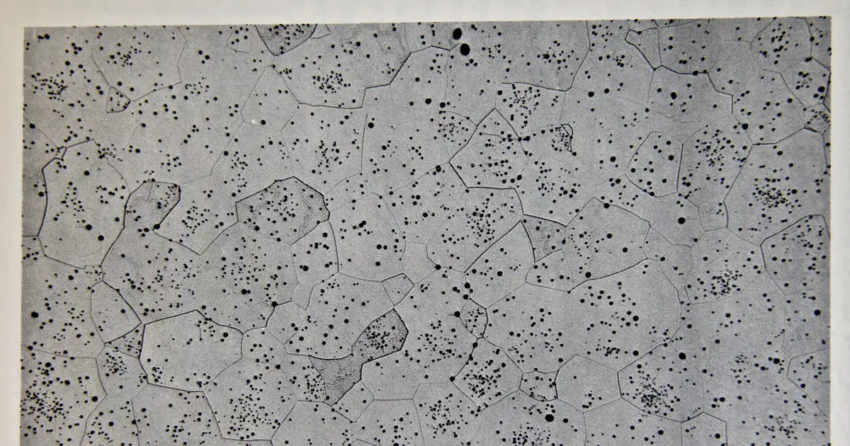
Etching chips means exposing the inside of a vacuum chamber to a plasma that is built to attack silicon, oxide and metal. The chamber walls, windows, rings and nozzles get attacked too. For years the standard answers were anodised aluminium, quartz and alumina. As feature sizes shrank and cleanliness requirements tightened, yttrium oxide, or yttria, moved into the most exposed positions.
This guide covers what makes yttria suitable, what makes it difficult and what a buyer should put on a drawing.
Why yttria resists plasma
Fluorine and chlorine plasmas react with most oxides. Alumina forms aluminium fluoride, which can be volatile or flaky. Quartz forms volatile silicon fluoride and erodes quickly. Yttria reacts with fluorine to form yttrium fluoride or an oxyfluoride, and that surface layer is stable, dense and slow to erode.
The consequences in a chamber are practical:
- Longer part life. Erosion rates in a fluorine plasma are much lower for yttria than for alumina or quartz in published tests.
- Fewer particles. A stable surface sheds less debris, so there are fewer defects on the wafer.
- Less chamber drift. Surface chemistry changes more slowly, which helps process repeatability.
Published erosion rate comparisons vary with plasma conditions, so no single ratio applies everywhere. The direction of the result is consistent, which is why yttria appears across several chamber parts. For context on where such parts sit in a tool, see ceramic parts in semiconductor equipment.
Typical properties
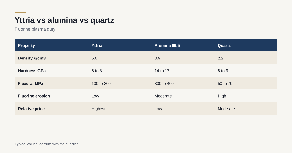
| Property | Sintered yttria | Alumina, 99.5 percent | Quartz |
|---|---|---|---|
| Density | About 5.0 g/cm3 | About 3.9 g/cm3 | About 2.2 g/cm3 |
| Hardness | Roughly 6 to 8 GPa | Roughly 14 to 17 GPa | Roughly 8 to 9 GPa |
| Flexural strength | About 100 to 200 MPa | About 300 to 400 MPa | About 50 to 70 MPa |
| Thermal conductivity | About 14 to 27 W/mK | About 25 to 30 W/mK | About 1.4 W/mK |
| Thermal expansion | About 7 to 8 ppm per K | About 7 to 8 ppm per K | About 0.5 ppm per K |
| Melting point | About 2400 degrees C | About 2050 degrees C | Softens near 1700 degrees C |
| Fluorine plasma erosion | Low | Moderate | High |
These are typical figures from published data. They depend on purity, density and grain size, so use the producer’s datasheet for design numbers.
What makes it difficult
Sintering. Yttria has a very high melting point and sinters only at high temperature, typically 1600 to 1800 degrees C or more, often with fine, high purity powder. Reaching full density without sintering additives is harder than for alumina. Additives introduce contaminants, which defeats the purpose in a chip tool. Producers use careful powder control and, for the best material, hot pressing or similar methods. See hot isostatic pressing for ceramics for one of the routes that closes final porosity.
Purity. Semiconductor use often calls for 99.9 percent or better and for tight limits on transition metals and alkali. The shop and the powder supplier must control them. A buyer should ask for the impurity analysis of the lot.
Strength. Yttria is soft and relatively weak. It chips at edges and corners, so designs add generous radii and chamfers. See corner radius and edge chipping.
Cost. Yttrium oxide powder is costly compared with alumina and the yield is lower. A sintered yttria part can cost many times the alumina equivalent.
Thermal behaviour. The expansion and the conductivity are similar to alumina, so thermal shock behaviour is similar, though the lower strength gives less margin. Handle heating and cooling ramps with care.
Sintered parts, coatings or both
Yttria in a plasma tool takes three forms.
- Bulk sintered parts. Rings, windows, liners and nozzles made entirely of yttria. No coating to peel, and surfaces can be reground. Highest cost.
- Thermal sprayed coatings. Yttria sprayed onto aluminium or alumina parts. Lower cost and flexible in shape, but coatings are porous and can spall.
- Deposited and dense coatings. Aerosol, vapour or ion-assisted deposition gives denser layers. Higher cost than spray and lower than bulk for large parts.
The choice depends on the part geometry, the budget and the plasma exposure. A flat focus ring in a harsh position favours bulk. A large complex liner favours coating. See also ceramic vs coated metal for the general trade-off.
How yttria parts fail in service
Understanding the failure modes helps set the specification.
- Surface roughening. Even a resistant material erodes slowly. Grain boundaries and any residual porosity erode faster than grain faces, so a coarse or porous body roughens sooner. This is why density and grain size appear on specifications.
- Fluoride layer growth and flaking. Over many hours the fluorinated surface thickens. If the layer cracks because of thermal cycling, flakes become particles. Smooth, dense parts with a tight bond to the fluoride layer do better.
- Thermal cracking. A ring or window heated by the plasma on one face and cooled from the other sees a gradient. With a modest strength, a crack can start at an edge or a hole.
- Contamination from the part itself. Impurities in the ceramic can leave the surface and land on the wafer. Purity and the cleaning route matter as much as the erosion rate.
Because yttria is soft, mechanical damage during handling is also a common cause of early removal. A chip on an edge can become a particle source even before the part has run a plasma hour.
Handling and packing
A yttria part for a chip tool should travel and be stored carefully.
- Pack in clean, low-particle bags with soft separators, double bagged if the cleanroom requires it.
- Keep parts away from hard contact. A part that touches another part in a tray can chip an edge.
- Handle with clean gloves. Skin oil and sodium on the surface can change the first plasma cycles.
- Record the lot number and keep the certificate with the part, so a field failure can be traced.
For general advice on safe transport of brittle parts, see packing and shipping ceramic parts.
A worked example
A fab uses an alumina focus ring around the wafer in an etch tool. The ring erodes, the etch rate at the wafer edge drifts and the ring is replaced every few hundred plasma hours. A yttria ring in the same position costs several times as much, yet it lasts longer in the same plasma, drifts less and generates fewer particles. Whether the swap pays off depends on how much each replacement costs in downtime and lost wafers. For a high-value process, the downtime saving can be larger than the price difference. For a low-value process, alumina may still be the better buy.
This is the right way to judge yttria: on cost per plasma hour and per wafer, not on the part price alone. Ask the shop for the lifetime data it has for the tool type, but treat any figure as indicative, since plasma conditions differ between tools and recipes.
Machining yttria
- Diamond grinding only. The sintered body is hard enough to need diamond. See how diamond grinding works.
- Light cuts. The low strength invites chipping, and shops use fine wheels and slow infeed on edges.
- Cleanliness. Parts must be cleaned to the semiconductor standard, often with controlled agents and in a clean environment. Agree the cleaning specification before ordering.
- Surface finish. Smoother surfaces erode more evenly. The roughness is often specified on the plasma-facing side.
- Tolerance. Ground faces can hold the same kind of tolerance as other dense oxides, within the limits the lower strength allows.
Checklist for the RFQ
- Purity level and impurity limits, with the analytical method.
- Density, as a percentage of theoretical.
- Plasma gas, power and the faces exposed.
- Surface roughness on the exposed side.
- Edge radius and chamfer.
- Cleaning and packaging specification.
- Whether a coating on another substrate is an acceptable alternative.
If you buy plasma-facing ceramics, describe the chamber duty in an RFQ and ask the shops to quote bulk and coated options.
Frequently asked questions
Why is yttria used in plasma etch equipment?
In fluorine and chlorine plasmas, yttria forms a stable fluoride or oxyfluoride surface layer that erodes slowly and sheds fewer particles than alumina or quartz. That keeps chamber parts in service longer and reduces contamination on the wafer.
Is a sintered yttria part better than a plasma-sprayed coating?
They serve different jobs. A sintered bulk part has no coating to peel and can be reworked, but it is expensive and limited in shape. A sprayed or deposited coating on aluminium or alumina is cheaper and can cover complex shapes, but it has a finite thickness and can spall.
Is yttria strong?
No. Its strength and hardness are well below alumina. Handle parts with care, avoid sharp corners and expect edge chipping to be a more frequent concern than with alumina.
Need a quote for this part?
Send the drawing. We match you with up to 3 shops that grind this grade and reply within 24 business hours.
Get matched with a ceramic shop